NINGBO CHIPEX SEMICONDUCTOR CO.,LTD
Add:No.18 Zhongheng Road,Huaxing District,Andong Industrial Park,Hang Zhou Bay New Zone,Ningbo
P.O:315327
Mail:sales@chipex.cn
Tel:(86)-574-63078606;
(86)-574-63078608-8858
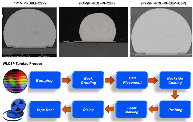
Wafer Level Chip Scale Packaging is different from the traditional chip package (Sawing before packaging and testing, and the volume will be increased at least 20% than the original chip). This latest technology is firstly film deposited on the wafer, then litho, electrochemical deposition, packaging and testing will be go on, at last been sawed into the same size die as the chip scale, without going through the wire and filling process, the chip size is almost the same as bare chip after packaging. Packaging efficiency close to 100%, in line with consumer electronics products’ market trend of light, small, short and thin, and has a large density, low induction, low cost, good heat dissipation and so on. The advantages of packaging are more obvious while wafer size increases and die size decreases.
| CSP Structure | PI Thickness |
UBM Thickness |
Other |
1P1M (PI+U+CSP) | 5um/10um | 8um | Min.Ball Pitch:0.3mm Min.Ball Size: 0.15mm Min.PI Opening:30um Min.Trace Line X Space:10X10um |
2P1M (PI+RDL+PI+CSP) | 1st PI 5um 2nd PI 10um | 8um | |
2P2M (PI+RDL+PI+UBM+CSP) | 1st PI 5um 2nd PI 10um | RDL:5um UBM:8um | |
3P3M (PI+RDL+PI+RDL+UBM+CSP) | 1st PI 5um 2nd/3rd PI 10um | RDL:5um UBM:8um |
Pitch (um) | Product Type | Bump Height(um) | Bump Diameter(um) | UBM Size(um) |
| 300 | 1P1M/2P2M | 100±20 | 180±20 | 180 |
| 2P1M | 100±20 | 165±20 | 160 | |
| 400 | 1P1M/2P2M | 195±20 | 270±20 | 240 |
| 2P1M | 200±20 | 260±20 | 210 | |
| 500 | 1P1M/2P2M | 235±20 | 320±20 | 280 |
| 2P1M | 235±20 | 310±20 | 240 | |
| 600 | 1P1M/2P2M | 280±20 | 370±20 | 320 |
| 2P1M | 280±20 | 360±20 | 300 |
Application:
IPD,PMU,Local Power,VCM Driver,Switch,Audio& Video,EEPROM,MEMS&Sensor,PA
