NINGBO CHIPEX SEMICONDUCTOR CO.,LTD
Add:No.18 Zhongheng Road,Huaxing District,Andong Industrial Park,Hang Zhou Bay New Zone,Ningbo
P.O:315327
Mail:sales@chipex.cn
Tel:(86)-574-63078606;
(86)-574-63078608-8858
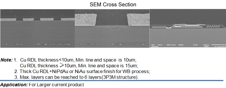
Redistribution Line changed the original design of the IC line contact I/O pads by through the wafer-level metal routing process and the bump process, so that IC can be applied to different packages. Wafer-level metal routing process is firstly the IC coated with an insulating layer of protection, and then exposed development to define new ways of the pattern, and then use the plating technology to create new metal lines to connect the original aluminum pad with the new convex block or gold pad, making a redistribution line. The metal lines of redistribution always are copper plating materials, also can be nickel-plated copper wire or nickel-palladium gold if needed. Thick copper structure will be the best choice for high-current and high-power devices due to its low resistance, high heat dissipation and low cost advantages.
The advantages of redistribution line are as follows: change the circuit I/O original design, increase the added value of the original design; increase the I/O spacing, providing a larger area of the bump, reducing the stress between the substrate and components to increase the reliability of components; replace part of the IC circuit design, accelerate IC development time.

